Nvidia admits that the projected performance gains are “CEO estimates” so the big question is still out there: what exactly can we expect from Pascal?
Despite Christmas just few weeks away, some from the PC gaming community are holding back the trigger for Nvidia Maxwell cards to cash in on a new line of GPUs powered by the highly-anticipated Pascal architecture coming this 2016. With CEO Jen-Hsun Huang saying that Nvidia Pascal, codenamed GP100, will be 10 times faster than Maxwell, its no wonder why.
Huang admitted though that the projected performance gains are “CEO estimates” so the big question is still out there: what exactly can we expect from Pascal? News about the Maxwell successor began in March 2014 when Nvidia official shared its GPU roadmap during the GPU Technology Conference (GTC). Now, new details about it were revealed during GTC in Japan. Here’s a wrap up of what we know about Pascal so far.
No more DDR5 VRAM

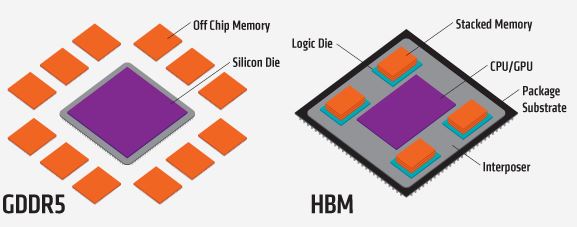
Instead, Nvidia will use the next-generation HBM2 memory standard for Pascal (3d ‘stacked’ memory). HBM, which stands for High Bandwidth Memory, was first introduced by AMD with the Fury X and its basically a new kind of memory. If you noticed with your DDR5 cards, its memory chips are soldered around the main chip. On the other hand, HBM memory chips can be stacked right next to the processor leading to more bandwidth, better power efficiency and overall faster performance.

Up to 32GB of RAM per GPU
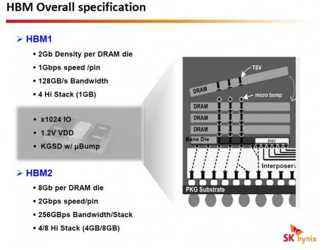
While AMD was first to market with this technology, they could only utilize HBM1 which has a 4GB VRAM limitation via single GPUs and 8GB with a dual card solution. HBM1 cards with 4 GB HBM with Team Red includes the Fury X, Fury, Nano and Fury X2.
Generation two or HBM2, allows Nvidia to double the effective speed per pin and higher memory densities. This means that GPU cards can have four HBM 2.0 chips, 4GB per chip, or four HBM 2.0 chips with 8GB per chip, creating a card with up to 32GB of VRAM.
Nvidia did confirm in GTC Japan however that upcoming Pascal cards will launch with 16GB but this capacity will most likely increase in the future. The need for this amount of VRAM is out for debate but as games get more and more demanding (looking at you 60fps 4k gaming!), it’s always a good idea for memory technology to be far ahead.
Will have 1TB/s of total bandwidth
Memory bandwidth is basically the speed of the video RAM – the amount of memory that can be used to process files in a second. It’s measured in gigabytes per second (GB/s). The more bandwidth you have, the faster the video card can draw higher quality images.
To give you an idea what 1TB/s of total bandwidth means, consider the Nvidia GTX 980ti and Titan X with each having a total memory bandwidth of 336.5 GB/s. That’s a huge bandwidth increase, two times what the AMD Fury X offers.
Nvidia Pascal is 16-nm based
Taiwan Semiconductor Manufacturing Company (TSMC) will be carrying out the manufacturing of Nvidia’s Pascal GPU, beating out a competing bid from Samsung and continuing a twenty-year collaboration between the two companies. This also means the introduction of TSMC’s 16 nanometer FinFET node.

Also called 16FF+ (FinFET Plus) technology, it pertains to the physical size of the GPU itself. Current GPU cards use 28nm fab process and, generally speaking, the more transistors you can fit on a card, the faster the card will be. The Nvidia GTX 980ti (6GB) is 28nm-based and boasts 8 billion transistors.
How about Pascal? Up to 17 billion transistors while maintaining a smaller physical size. According to TSMC, their 16-nm process can also deliver above 65 percent higher speed, around 2 times the density, and 70 percent less power compared to its 28nm counterpart.
Will support NVLink
Pascal will be the first GPU in the world to adopt NVLink, Nvidia’s attempt to connect a PC’s processors – CPUs and GPUs – so they can exchange data 5 to 12 times faster.

A typical system has one or more GPUs connected to a CPU using PCI Express. And even at the fastest PCIe 3.0 speeds (8 Giga-transfers per second per lane) and with the widest supported links (16 lanes), PCIe greatly limits the real bandwidth available between the CPU and its system memory. NVLink will provide between 80 and 200 GB/s of bandwidth, allowing the GPU full-bandwidth access to the CPU’s memory system. We can only begin to imagine how that will impact multi-GPU setups.
[youtube https://www.youtube.com/watch?v=RBf8FLS6q8E&w=560&h=315]
Now, explaining how Nvidia will do that exactly is a mouthful so here’s a link to an awesome blog post from them explaining the whole thing.
On track for 2016 release
Arguably the most important bit of news is will Pascal be launched in 2016. It’s a yes, according to 3D Center.org, which posted a screenshot from Zauba, India’s import and export database, showing that at least 9 engineering samples have been shipped from Taiwan to Bangalore, India for testing and evaluation for mass production. Industry observers estimate that Nvidia GPUs running on Pascal will be launched around second quarter of 2016.


Great article. Well elaborated and helpful!